 |
 |
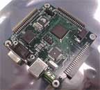
Develop custom signal processing applications on FPGA using this generic development platform
Xilinx Virtex-II XC2V1000-4 FPGA features 1 million system gates, 720Kbit of dual port memory, 40 18x18 multipliers
USB 2.0 interface supports signaling rates of 480 Mbits/s (High Speed) and 12 Mbits/s (Full Speed). Typical sustained data throughputs are 85 Mbit/s (HS) and 6.5 Mbit/s (FS)
Modules can be stacked for large design development
FPGA configuration remains in non-volatile flash memory and is automatically reloaded at power up
Graphical User Interface is used for remote monitoring and control over simple serial link. This includes loading FPGA configuration file into flash. No special cable nor serial EPROM is needed
This module is interface compatible with other pre-programmed ComBlock modules
120 MHz maximum clock rate (typ.)
 |
 ComScopeenabled: key internal signals can be captured in real-time and displayed on a host computer ComScopeenabled: key internal signals can be captured in real-time and displayed on a host computer |
 |
Connectorized 3”x 3” module for ease of prototyping. Standard 40 pin 2mm dual row connectors (left, right, bottom). Single 5V supply with reverse voltage and overvoltage protection.
See Also the COM-1200 for larger FPGA, USB 2.0, Integrated analog front-end (A/D and D/A converters)
|
| |
| Input |
Output |
| Most ComBlocks |
Most ComBlocks |
|
|
 Home
Home